
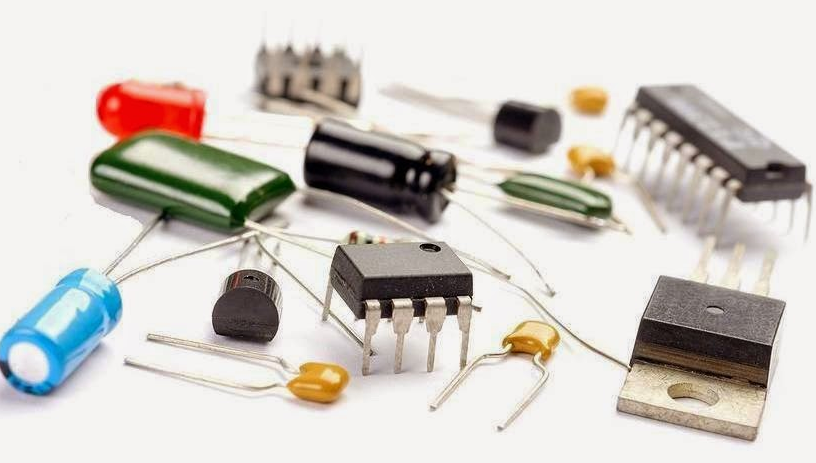
There are semiconductor devices in television, radio, mobile phones, and other electrical or electronic products. Unlike complete electricity conductors like aluminum, copper, and steel, the materials used in semiconductor devices can partly conduct electricity.
A semiconductor falls between a conductor and an isolator somewhere. For this purpose, Integrated Circuits are widely used for producing them. Silicon is an excellent example of semiconductor material. For different purposes, this is the most commonly used material in the microelectronics industry. Its low price and availability are one of the primary factors.
What is Semiconductor Test equipment (IC tester)?:
Semiconductor Test Equipment (IC Tester) or Automated Test Equipment (ATE) is a system for delivering electrical signals to a semiconductor device for testing to compare the output signals with the expected values if the device is operating as specified in its design specifications.
Testers are categorized roughly into logic testers, analog testers, and memory testers. IC testing is usually performed at two levels: the wafer test (also referred to as die sort or probe test), which tests wafers, and the package test (also referred to as the final test) after packaging.
When is Semiconductor Test done?:
From prototyping to end-product maintenance, semiconductor testers are used throughout the product life-cycle. The first test that takes place is referred to as the characterization test of the prototype. Following the first production, the second test takes place. In the production process, it primarily identifies flaws. The intermediate and final production tests are the next two tests.
Manufacturing semiconductors:
There are several main processes when it comes to the manufacture of semiconductor devices. The primary ones are deposition, patterning, removal, and alteration of properties for electrical purposes. Affidavit refers to another substance being added or coated onto the substrate. Technologies such as physical vapor deposition or PVC and chemical vapor deposition or CVD could be used to do this.
Removing of semiconductors:
Dry or wet etching methods can be used in the removal process to remove material from the semiconductor substrate. Patterning is the substrate’s forming or reshaping. Lithography is one of the prevalent techniques. Ion implantation is one of the most common electrical property modification techniques. Ions are implanted on the substrate, as its name indicates, to modify its physical properties.
Conclusion:
To summarize, in all the current electrical or electronic products on the market, semiconductor devices are used. Many steps are involved in the manufacturing procedures for these devices. Wafer processing, die preparation and IC packaging are the major processes. Integrated circuit testing is carried out as a final inspection before packing and delivery to a customer to check all chips and substrates’ overall functions. Integrated circuit testing is carried out as a final inspection before packing and delivery to a customer to inspect all chips and substrates’ general operations.
These semiconductors have now become a part of our lives, and we can’t survive without these devices. Whether you’re talking about lifeline computers or telephones that keep us connected, they all have semiconductors in one form or the other.